GRUPO DE MICROELETRÔNICA (GMICRO)
Pesquisa Em Atividade
Contato:
batista@inf.ufsm.br (55) 3220-9423 Prédio:7 – CTMaterial Adicional
CADENCE UNIVERSITY PROGRAM 
Cadence is a registered trademark of Cadence Design Systems, Inc., 2655 Seely Avenue, San Jose, CA 95134.
This page was last updated on October 22nd, 2020.
TEACHING ACTIVITIES
Cadence® design automation tools are used as a major component in eight undergraduate and graduate courses at the UFSM:
Undergraduate Courses (Electric Engineering and Computer Science):
Design of Digital Integrated Systems(60 hs) – ELC 1054 (60 hs): The CMOS switch, levels of abstraction in digital design, CMOS inverter, CMOS technology basics, design tools, technology files, layout rules, design techniques, introduction to VLSI design.
Design of Analog Integrated Circuits I – ESP1017 (60 hs): Physics of semiconductor basics, MOSFET structure, current x voltage characteristic, small-signal model, second-order effects, single-ended stages, differential stages, current mirrors, operational amplifiers, op-amp design basics, simulation practice.
Design of Analog Integrated Circuits II – ESP 1035 (60 hs): Frequency response of amplifiers, noise analysis, feedback and frequency compensation, case studies in analog design: low power design, switched capacitor circuits, layout techniques.
Analog to Digital Converters – ELC 1063 (60 hs): A/D conversion fundamentals; case studies: system, electrical and physical level design.
Graduate Courses (Electric Engineering and Computer Science):
Introduction to VLSI Design – ELC 891 (60 hs): MOS transistors and simple logic gates, design rules, electric simulation, performance estimation, symbolic design, combinational logic blocks (ROM, PLA), memory blocks, project styles (gate array, standard cells, full custom), introduction to automatic synthesis.
Design of Digital VLSI Systems – ELC 904 (60 hs): System specifications, microprocessor architectures, design methodologies, hardware/ software co-design, high-level description languages, case studies – design of processor blocks.
Design of Analog Integrated Circuits I – ESP1038 (60 hs): Design cases of analog CMOS integrated circuits.
Design of Analog Integrated Circuits II – ESP 1039 (60 hs): Design cases of analog, and mixed-signal CMOS integrated systems.
CHIP DESIGNS
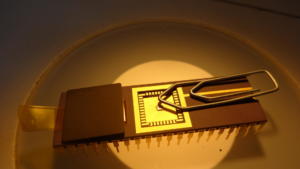
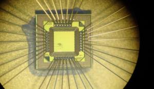
Design of digital Sobel Filter fabricated through MOSIS (undergraduate course ELC1054): This circuit performs image processing within an edge detection algorithm and was sent for fabrication using a GlobalFoundries 130 nm process.


RESEARCH ACTIVITIES
Design of an Implantable Neural Interface
Type: Applied Research
Areas: Microelectronics, instrumentation, Biomedical Engineering.
Begin: January/2015
Participants: UFSM, UCBM (Rome, IT.)
Funding: MCT, CNPq
Abstract: Design and testing of a wireless implantable system for both acquiring and applying signals from/into peripheral nerves. The system comprehends: implanted and external blocks for: signal conditioning, data conversion, stimulator, control, energy, and communication.
Design Tools: Virtuoso, Innovus, Spectre, Allegro/OrCad.
Design of an Analog to Digital Sigma Delta Converters for programmable base-band using Switched Current techniques
Type: Applied Research
Areas: Microelectronics, Analog, and Mixed Signals
Begin: Mar/2009
Participants: UFSM/Gmicro/PPGEE
Funding: FAPERGS/UFSM
Abstract: This project aims to design an ADC Sigma Delta type, which meets the standards GSM / WCDMA / WLAN capable of being managed in accordance with the required operating bandwidth. The approach of constructing circuits will be using the technique of switching current (SI). The technology to be used preferably will be available in the manufacturing process CEITEC.
Last modified on October 22nd, 2020. Page maintained by Leonardo Londero de Oliveira (leonardo@ecomp.ufsm.br).


